

Samsung Electronics will make the base die for Nvidia's custom high-bandwidth memory, NVHBM, on TSMC's 3nm process, the Seoul Economic Daily reported on October 18, citing industry sources. Reuters picked up the report the same day. If it holds, it is the first time Samsung and TSMC have worked together at the HBM manufacturing stage, and it means Samsung gives up its build-everything-in-house model for its largest memory customer.
The report rests on unnamed sources. Nvidia, Samsung and TSMC have not announced the arrangement.
What the report says
According to the Seoul Economic Daily, Nvidia asked all three NVHBM suppliers, Samsung, SK hynix and Micron, to do two things:
- Make the NVHBM base die on TSMC's 3nm process.
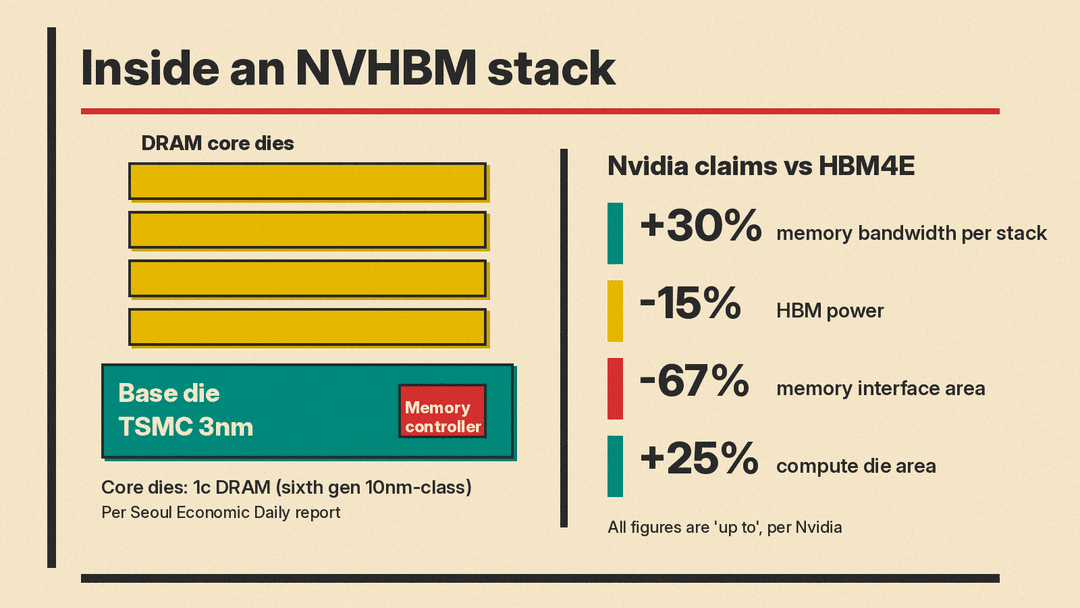
- Make the stacked DRAM core dies on the same DRAM generation, known as 1c (the sixth generation of 10nm-class DRAM).
The paper says NVHBM is based on the HBM4E architecture. Nvidia's stated reason, as reported, is consistency. When each supplier builds the base die its own way, one Nvidia design does not behave the same across all three. A common recipe also means Nvidia validates one product instead of three variants.
Samsung's Device Solutions division, which also runs its foundry business, accepted the request after an internal review, the paper said.
Why the base die matters
An HBM stack is a pile of DRAM dies sitting on a logic die, the base die. In standard HBM the memory controller lives on the GPU or accelerator. NVHBM moves that controller into the base die and adds a custom physical interface, according to Nvidia's technical blog from August 26. That makes the base die a real piece of logic silicon, which is why the process node matters.
Nvidia's own claims for NVHBM, compared with standard HBM4E:
- Up to 30% more memory bandwidth per stack.
- Up to 15% lower HBM power.
- Up to 67% less area for the memory interface and support circuits, which Nvidia says frees up to 25% more compute die area.
Nvidia offers NVHBM through NVLink Fusion, its program for hyperscalers that build their own accelerators and want to plug them into Nvidia's rack and networking stack. So the base die decision affects custom chips from Nvidia's partners, not only Nvidia GPUs.
What Samsung keeps
The change is narrow. Samsung will keep its turnkey approach for standard HBM, the paper said. Its HBM4, in mass production since earlier this year, and HBM4E, now in mass-production validation, both use Samsung's own 4nm foundry process for the base die. The core dies come from 1c lines at its Hwaseong and Pyeongtaek campuses.
Samsung will also keep the turnkey model for custom HBM it supplies to other customers, including AMD. And it has not given up on NVHBM base dies at its own fabs. An industry official told the paper Samsung is validating its foundry for this part "in case NVHBM demand exceeds TSMC's production capacity." TrendForce, citing the Seoul Economic Daily, says that backup is Samsung's 2nm (SF2) process.
TrendForce also cites industry yield estimates: above 90% for TSMC 3nm, versus around 60% for Samsung SF2. Those are secondhand estimates, not company figures.
Why it matters
Control is moving to the buyer. HBM used to be a product memory makers designed and sold. With NVHBM, Nvidia sets the base die design, the foundry, and the DRAM generation, and the three memory makers build to that spec. DigiTimes described it as control over how HBM is built shifting from memory makers to their largest customer.
Samsung's pitch gets weaker where it counts most. Samsung has sold its ability to make DRAM, logic and packaging under one roof as an HBM advantage. For Nvidia's custom memory, that advantage no longer applies. It still applies for AMD and others.
TSMC 3nm gets another demand line. TSMC said at its October 15 earnings call that 3nm was 33% of third-quarter wafer sales, its largest node, according to TrendForce. The same report says TSMC plans another 3nm fab in Tainan for mass production in the first half of 2028. NVHBM base dies from three suppliers add to a node already shared by AI accelerators and phone chips. That is the scenario Samsung's own-fab backup is meant for.
Fewer variants, simpler qualification. For accelerator builders, one base die made one way across three suppliers should make memory qualification faster and multi-sourcing easier. That is Nvidia's stated goal, and it is the reason a memory maker would accept a rival foundry inside its product.
What to watch: any confirmation from Nvidia or Samsung, the first NVHBM sample and qualification dates, and whether Samsung's 2nm backup reaches production.
Sources
- Seoul Economic Daily: Samsung to Tap TSMC for Nvidia's Custom HBM Base Die
- Reuters via The Star: Samsung to use TSMC technology for Nvidia's next-generation memory chips
- TrendForce: NVIDIA Reportedly Pushes TSMC 3nm NVHBM Base Dies for Samsung, SK hynix, Micron
- DigiTimes: Nvidia's custom HBM pulls Samsung onto TSMC's 3nm process, report says
- NVIDIA Technical Blog: NVLink Fusion Brings NVHBM to Next-Generation AI Infrastructure
