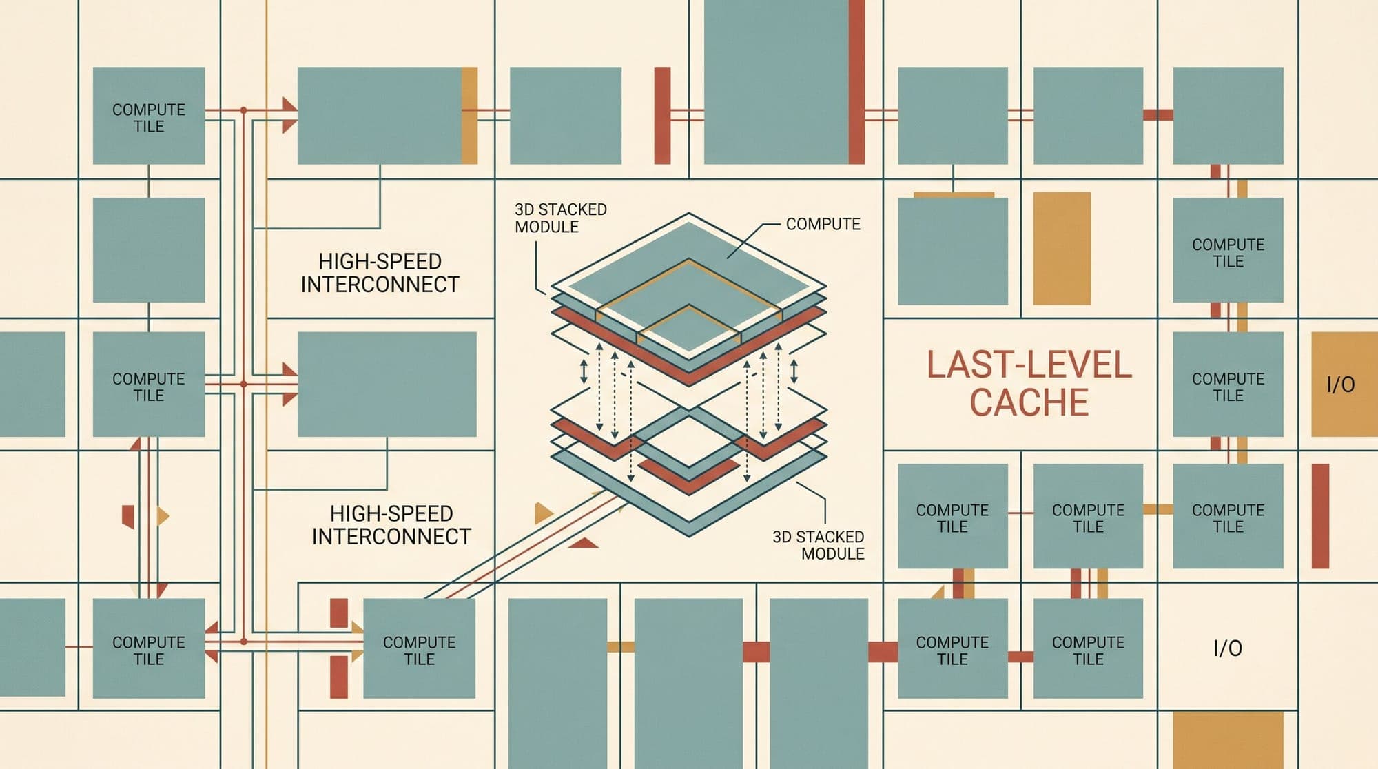
At the Hot Chips 2026 symposium, Intel unveiled the microarchitectural details for its next-generation data center platform, Xeon 7 (codenamed Diamond Rapids). Scheduled for production release in 2027, the flagship processor features up to 256 performance cores, 1.28GB of Last-Level Cache (LLC), and native FP8 support within its Advanced Matrix Extensions (AMX).
The design marks a shift in Intel's high-performance server strategy, dropping Simultaneous Multi-Threading (SMT) entirely in favor of dedicated physical cores targeted at enterprise AI orchestration and latency-sensitive workloads.

Modular 3D Chiplet Disaggregation
Diamond Rapids transitions from the 2.5D planar tile structures used in Sapphire Rapids and Granite Rapids to a full 3D stacked topology. The flagship package integrates 22 discrete silicon dies fabricated across two Intel Foundry process nodes:
- 16 Core Compute Dies (18A-P node): Each core die houses 16 Panther Cove performance cores (P-cores), aggregating to 256 physical cores per socket.
- 4 Compute Base Tiles (Intel 3-T node): The core dies sit atop four active base tiles via Foveros Direct 3D hybrid bonding. Each base tile incorporates 320MB of shared L3 cache, delivering a cumulative 1.28GB Last-Level Cache pool across the processor.
- 2 Fabric Hub Tiles (Intel 3 node): Connected to the compute base via copper substrate links, these tiles manage memory controllers, coherency routing, and high-speed I/O interfaces.
By decoupling the dense execution units from the shared cache and I/O infrastructure, Intel concentrates high-cost 18A-P lithography exclusively on the execution pipelines while using mature Intel 3 processes for bulk SRAM and interface circuits.
Dropping SMT for Deterministic Agentic Compute
Unlike prior Xeon generations and competing server chips such as AMD's EPYC Venice architecture, Diamond Rapids completely removes Hyper-Threading. The flagship configuration provides 256 physical cores and 256 logical threads per socket.
Intel engineers highlighted several architectural trade-offs behind this decision:
- Elimination of Resource Contention: SMT architectures share execution ports, register files, and L1/L2 caches between co-located threads, introducing tail-latency spikes when running unpredictable, branch-heavy code.
- Deterministic Execution in AI Agent Frameworks: Agentic orchestration, code execution sandboxes, and vector retrieval pipelines demand consistent per-thread throughput rather than aggregate throughput compromised by thread stalling.
- Silicon Area Optimization: Stripping thread contexts, reorder buffer duplications, and architectural state registers frees die area for expanded vector/matrix ALUs and larger private L2 caches.
Upgraded Matrix Acceleration: FP8 AMX and AVX 10.2
To address local inference, data prep, and embedding extraction directly on host CPUs, Intel integrated substantial enhancements into the vector and matrix execution blocks:
- FP8 Advanced Matrix Extensions (AMX): Diamond Rapids introduces native hardware execution for standard 8-bit floating-point formats (E4M3 and E5M2). This doubles theoretical matrix multiply throughput compared to BF16/FP16 pipelines and matches common quantization standards used in frontier model serving.
- AVX 10.2 Support: The Panther Cove cores implement the full AVX 10.2 instruction set with 512-bit vector widths, optimizing tokenization routines, softmax layers, and non-linear activation functions.
Memory Subsystem and High-Speed Interconnects
To feed 256 cores and 1.28GB of L3 cache without starvation, Intel redesigned the memory and peripheral controllers:
- 16-Channel Memory Controller: Supports standard DDR5-8000 speeds, scaling up to 12,800 MT/s when paired with Multiplexed Ranked DIMMs (MRDIMMs).
- 128 PCIe 6.0 and CXL 3.0 Lanes: Provides high-bandwidth interconnectivity for dense accelerator topologies, enabling low-latency cache-coherent memory sharing across CPU-to-GPU clusters.
Positioning in the AI Systems Stack
While specialized GPUs and custom ASICs remain the primary compute engine for large-scale model pre-training and dense token generation, the server CPU's role has expanded in agentic AI deployments. Host processors handle high-throughput context window preparation, tool-call validation, graph database traversal, and dynamic model routing.
With 1.28GB of shared cache, 16 memory channels, and 256 deterministic execution pipelines, Diamond Rapids is engineered to minimize host-side bottlenecks in next-generation inference clusters.
Sources
- ServeTheHome: Intel Diamond Rapids the 2027 Intel Xeon at Hot Chips 2026
- TrendForce: Intel Unveils Three AI Architectures at Hot Chips 2026
- TechTimes: Diamond Rapids Disclosed: Intel Xeon 7 Packs 256 Cores and Gigabyte Cache, Drops SMT
- StorageReview: Intel Hot Chips 2026: 256-Core Diamond Rapids, Crescent Island With 480GB for Inference